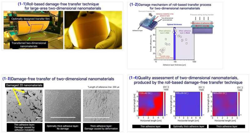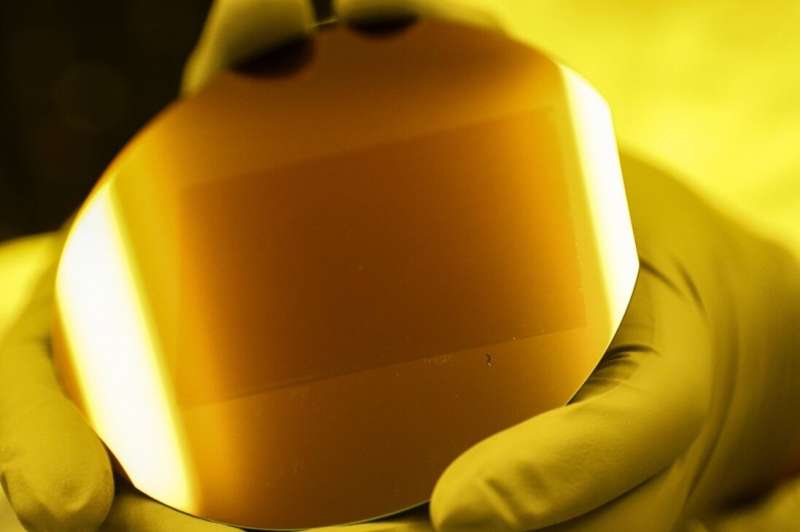
The Korea Institute of Machinery and Materials (KIMM) under the Ministry of Science and ICT developed a roll-based damage-free transfer technique that allows two-dimensional (2D) nanomaterials to be transferred into wafer scale without damage. The proposed technique has a variety of applications from transparent displays and semiconductors to displays for self-driving cars, and is expected to accelerate the commercialization of 2D nanomaterial-based high-performance devices.
Dr. Kwang-Seop Kim, principal researcher of the Department of Nano-Mechanics at KIMM, succeeded in developing a technique of transferring 2D nanomaterials, as thin as 1/50,000 of a strand of hair, to a substrate of at least 4 inches (approx. 10 cm) without damage.
The roll-based transfer is a process in which 2D nanomaterials on a transfer film are transferred to a desired substrate. It is a highly efficient technique that enables large-area continuous transfer of nanomaterials, similar to paper printing.
The transfer process involves nanomaterials on a transfer film (A) and a target substrate (B). In roll transfer, the nanomaterials are transferred to B when A is rolled onto B. This is similar to the process of transferring a tattoo onto skin using a tattoo sticker. The sticker plays the role of the transfer film, the tattoo represents the 2D nanomaterials, and the skin is the substrate.
The key point in the proposed technique is to identify two different types of the damage mechanisms in relation to the deformation of adhesive layer in the transfer film through computer simulation and experiments. The team optimizes the thickness of the adhesive layer to minimize the deformation of the adhesive layer during the transfer process, leading to achieve the damage-free transfer of large-area 2D nanomaterials.

The team discovered the principle behind the damage-free transfer of an extremely thin tattoo to skin through optimizing the tattoo sticker.
The technique can be utilized in the roll-based transfer process for the production of 2D nanomaterial-based flexible transparent displays and transparent semiconductors, decreasing the damage in 2D nanomaterial down to 1% compared to the existing 30%.
Principal researcher Kwang-Seop Kim said, "Our technique of transferring large-area 2D nanomaterials and micro-devices without damage to substrates will significantly lower manufacturing costs of wearable devices, flexible transparent displays, and high-performance bio/energy sensors, thus accelerating the commercialization of related applications. We also expect to see new businesses across industries from next-generation semiconductors to future vehicles."
Explore further
Provided by National Research Council of Science & Technology
Citation: Fast, affordable solution proposed for transparent displays and semiconductors (2021, May 17) retrieved 17 May 2021 from https://ift.tt/3fqqN5l
This document is subject to copyright. Apart from any fair dealing for the purpose of private study or research, no part may be reproduced without the written permission. The content is provided for information purposes only.
Fast, affordable solution proposed for transparent displays and semiconductors - Phys.org
Read More
No comments:
Post a Comment